MOSFET Control
My notes and practical implementations of circuits which leverage Mosfets. All of the following terminology only concerns N-type enhancement MOSFETS. These are by far the most common and useful. The other types are more or less just flipped versions.
Basics
A MOSFET is just a transistor with a simple quirk - the gate is electrically isolated from the rest. Effectively no current flows into the gate from the control line. And as long as the gate voltage is sufficiently high relative to the source (Vgs) then the resistance of the MOSFET from drain to source (Rds,on) will be on the order of milliohms.
Thermal Calculation
The thermal calculation for a MOSFET can be pretty simple if you are ok with being a bit fuzzy and don't intend to drive them to the limit. MOSFET datasheets usually specify:
| RθJC | Thermal resistance junction-to-case. | °C/W |
| RθJA | Thermal resistance junction-to-ambient. | °C/W |
| TJ, max | Maximum junction temperature. | °C |
There are two thermal cases to consider:
- Ambient heat dissipation.
- Heatsink-driven heat dissipation.
These two cases represent the bookends of possible heat dissipation for the MOSFET. At worst, the MOSFET simply dumps heat to the ambient environment, which includes both the air and the PCB itself. In this case, RθJA is dominant. At best, the MOSFET's case is perfectly connected to a heatsink that maintains a perfect temperature and only the resistance between the junction and the case (RθJC).
The ambient case is often unreachable as manufacturers tend to measure this number with PCB's that are large and unheated by other electrical signals. The rule of thumb is to use values about 50% higher for RθJA for this reason. It's also good practice to use pessimistic values for ambient temperature and stay well away from TJ, max.
Ambient Case
By combining ohms law with the thermal resistance and rules-of-thumb, the following equation results for maximum current flow in the ambient case:
I = math.sqrt(((TJ - 30) - TA)/(Rds*R0JA*1.5))
TA refers to ambient air temperature.
Heatsink Case
The heatsink case is a little trickier. Thermal resistances are available for the heatsink, they can be combined in series to form the following:
I = math.sqrt(((TJ - 30) - TA)/(Rds*(R0JC + RTC + RHS)))
TA refers to ambient temperature, RTC to contact thermal resistance, and RHS to heatsink thermal resistance..
Good quality heatsinks for the TO-220 style of MOSFET have resistances on the order of 4 °C/W in natural convection, dropping down to around 1 °C/W in forced air.
Praxis
The IRFZ44NPBF is a strong, quality through-hole TO-220 style MOSFET. The rest of this section will be concerned with the pragmatics of driving this MOSFET as a switch.
The IRFZ44NPBF has the following key characteristics:
| Parameter | Value | Notes |
| VDSS max | 55V | Voltage drain to source. |
| ID max | 49A | Continuous drain current, VGS=10V. Higher if pulsed. |
| VGS max | 22V | |
| VGS(th) | 2 - 4V | But for low resistance must be 10V |
| RDS(on) | 17.5 mΩ | At VGS=10V |
| RθJC | 1.5°C/W | Junction to case thermal resistance. |
| RθJA | 40°C/W | Junction to ambient thermal resistance. |
| TJ, max | 175°C | Max operating junction temperature. |
Use With 3.3v Logic
Most thru-hole MOSTFET's measure RDS,on at Vgs = 10V, so a smaller transistor must be used to turn one fully on with logic voltages like 5V or 3.3V. The venerable 2N3904 has a DC gain of 30 to 100 depending on input current and is useful in such situations.
In order to use the 2N3904 to switch the MOSFET we want to run it fully saturated, meaning the actual collector current iC, actual is less than the theoretical collector current iC, th that would be possible given the gain times the base current iB. When the 2N3904 is fully saturated, it has a voltage drop VCE(sat) of 0.3V at most.
If we form the following circuit and use a VCC of 12V:
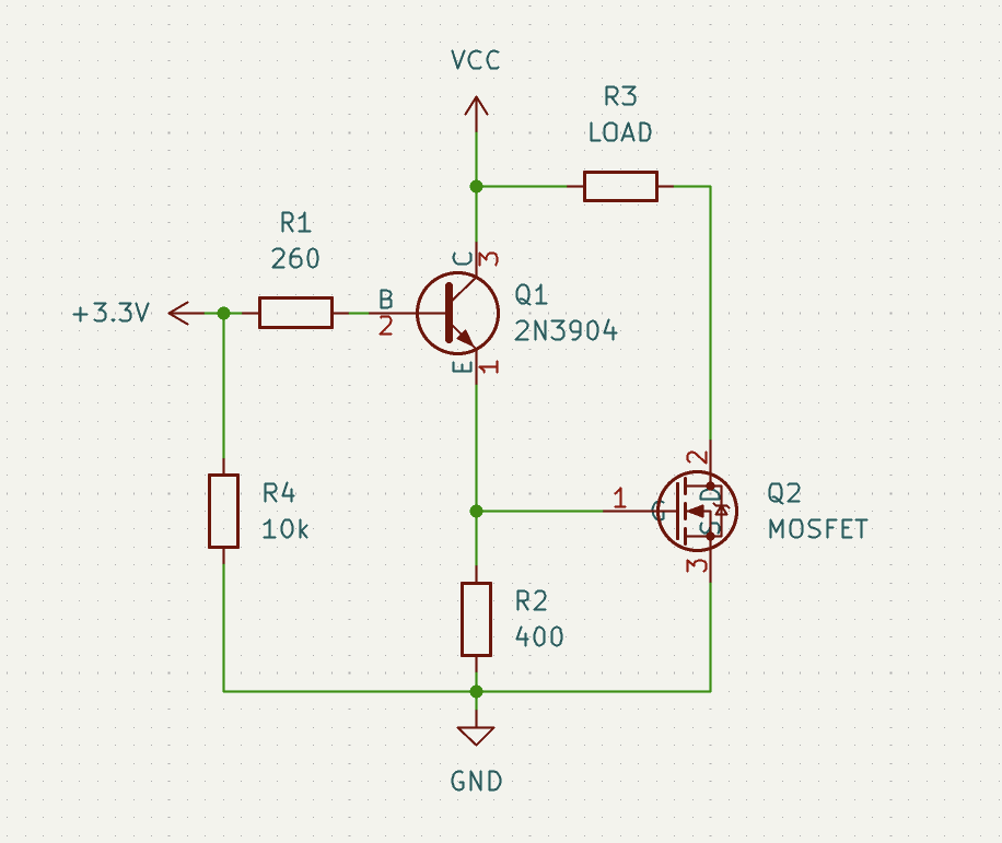
The current into the collector iC should be only 30mA and the current into the base a mere 5mA. That's still well within saturation ranges. A 12V signal is applied to the gate of the MOSFET. About 0.3W is used and turned into heat.
Hazards
- Body Diode
- A MOSFET acts like a switch from drain to source. However, source to drain acts like a diode with some voltage drop no matter what state the gate is in!
- Inductive Loads
- When driving an inductive load, voltage is still created by the load when power is cut off. This voltage can spike and destroy the MOSFET. Usage of a diode will shield the MOSFET from this problem. See the Inductive Loads Require a Diode section of the spencekonde guide for more info.
- Floating Capacitance
- The gate of a MOSFET can 'float' with electrical noise and become partially open, similar to how a GPIO input can return random data if it is not pulled down. The answer, of course, is to always put a pulldown on the gate of a MOSFET.
- Gate Resistors
- It is wise to place a resistor in series with a gate. This ensures the capacitance of the MOSFET can never drive voltage back into the microcontroller and damage its sensitive electronics.